EUROLAB's expertise in electronic failure analysis is to increase efficiency, determine the root cause of failure, predict product life expectancy, increase reliability and improve performance in integrated circuits (ICs), printed circuit boards (PCBs) and passive surface mounted devices. available.

Electronic Error Analysiscan provide detailed information about the performance of materials and devices in intended end use applications. When a device or material does not meet performance expectations, an electronic error analysis should be performed to identify the underlying cause of failure. The main reason is that the information presented in the electronic error analysis will allow the product designer, manager, test and process engineers or end user to identify the design, selection, test and process deficiencies. Suggestions for corrective actions from the failure analysis report can then be evaluated and implemented to improve product reliability and performance. By carrying out a neutral analysis by an independent testing laboratory, the responsibility of a failed device or material can be turned into an asset, which can lead to the production of higher quality products.
Ball Cutting and Die Cutting: In the ball cutting test, a mechanically driven wedge is used to cut solder balls from the BGA packages or solder bumps from the flip chip die. The ball cutting results provide information on solder-pad bond quality, which is directly related to the reliability and long-term performance of the solder joint. High voiding content, improper reflow profiles, contamination / cleaning problems, or improper coating of substrates / PCBs can lead to solder joint defects. Determination of the shear strength of solder joints is a qualitative method to determine the strength of the joint after reflow or assembly. Die Cutting can be performed on a variety of packages, including chip chips, direct fastening die or decapsulated plastic packages. Die cutting can give information about the quality of the die insertion bond to the back of the mold and inside the package or determine the mechanical strength of the flip chip bumps.
Curve Trace: Curve Trace is often used to determine the IV curves of a device. LRC meters are used to determine the electrical performance of common sense.
Decapsulation (De-Cap) - Jet-etch and acid: Decapsulation is the process of unpacking the mold compound from an integrated circuit or other plastic packaging to reveal the silicone mold inside. The process typically does not affect the electrical performance of the device, but requires visual inspection of the mold for failure analysis or EOS (electrical overstress), mold cracking, pad cratering, mold mold serialization, lot numbers, date codes or other information contained in the mold itself. Two common methods are used to decapulate devices. The jet-etch process uses a machine that pulls a heated stream of acid up the package, lifting the mold compound. The process induces minimal heat into the package and can be performed on devices such as BGA that require the solder to remain intact. Acid etching is a process that uses a hot plate and the part where the acid is removed is heated. The heated acid opens the mold for visual inspection, removing the mold compound.
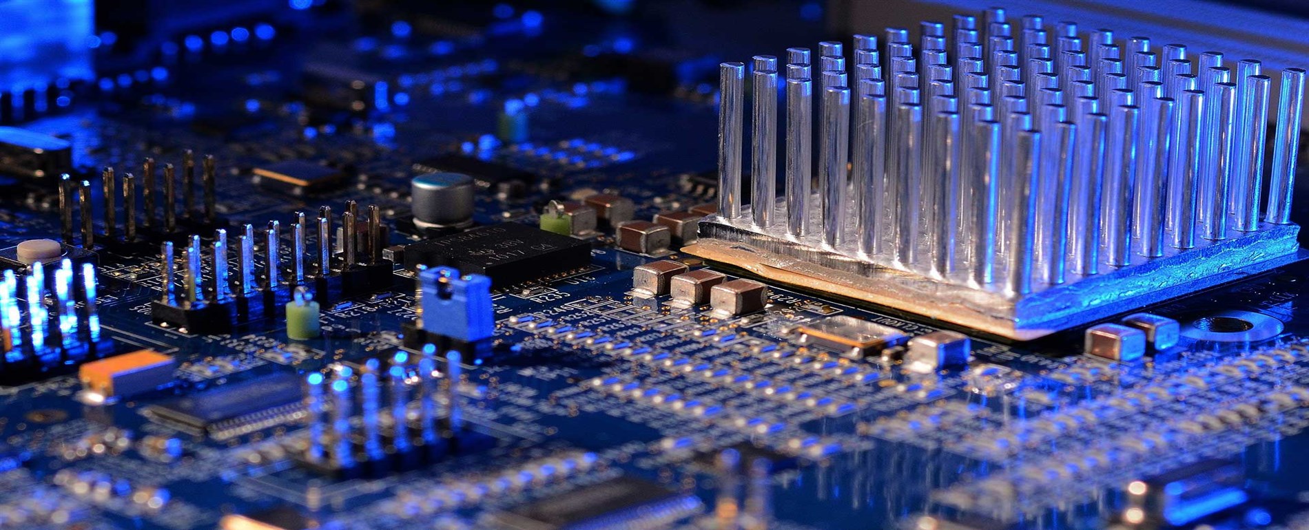
Electrical Characterization: Electrical Characterization is the key tool to characterize and verify the electrical performance of the devices under test, whether they are hidden surface mount devices, ICs, SOC, resistor networks or assemblies. Electrical characterization can be used to isolate a particular anomaly within the assembly and allows a more accurate analysis of a fault. Electrical characterization can be further improved to provide detailed performance data by applying external stress such as temperature, vibration or humidity.
Microsectional Analysis (Cross Section): Microsectional Analysis remains the most widely accepted method to analyze PCB / PWB plate integrity. It is a combination of different types of materials such as PCB, glass, aramid fiber, kapton, copper, acrylic adhesive, epoxy, polyimide, Teflon and solder. Each of these materials has a different relative hardness and when combined with that of the mounting medium, such as epoxy or acrylic, PCB microscopy is one of the most difficult to perform.
Scanning Acoustic Microscopy (CSAM): Scanning Acoustic Microscopy, also known as C-SAM or Acoustic Micro Imaging, or AMI, is its ability to find hidden flaws in assemblies and materials that may occur during manufacturing or environmental testing. Defects such as delaminations, voids and cracks can be identified and analyzed more effectively than other examination methods using Acoustic Microscopy.
solderability: Solderability testing method provides optional conditions for preconditioning and soldering to evaluate the solderability of instrument pack terminations. It provides procedures for immersion and solderability testing of hole, axial and surface-mounted devices, and surface-mount process simulation testing for surface-mounted packages.
To get an appointment, to get more detailed information or to request an evaluation, you can ask us to fill in our form and reach you.
EUROLABreporting and certification activities, United Accreditation Foundation (UAF), Turkish Accreditation Agency (TÜRKAK) ve Enterprise Accreditation Foundation (EAF) based on the accreditation provided by the accreditation body. The Enterprise Accreditation Foundation (EAF) accreditation body is also a signatory of the United Nations (UN GLOBAL COMPACT) organization.