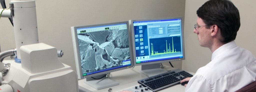

Scanning Electron Microscopy / Energy Distributor X-Ray Spectroscopy (SEM / EDS) protocol, It is a well established and accepted protocol for printed circuit boards (PCB), assemblies (PCAs) and electronic components (BGA, capacitors, resistors, inductors, connectors, diodes, oscillators, transformers, IC, etc.). Unlike normal optical microscopy, SEM / EDS allows for more detailed "inspection" of the analyzed areas.

Scanning Electron Microscopy (SEM) allows visual observation of an area of interest with the naked eye or completely different from a normal optical microscope. SEM images show simple contrasts between organic-based and metallic-based materials and therefore provide a large amount of information about the area being examined instantly. Energy Distributor X-Ray Spectroscopy (EDS), also sometimes called EDAX or EDX, can be used to obtain semi-quantitative basic results about very specific places of interest.
Simply put, SEM allows areas of interest to be studied at extremely high magnifications. Unlike normal optical microscopy, SEM produces high-resolution and detailed depth-of-field images. For example, surface structures, general abnormalities and areas of contamination can be easily identified and then isolated for further analysis if necessary.
A sample containing its interests and regions is placed in the vacuum chamber located under the SEM column. An electron source located at the top of the column produces electrons that pass through the column and form on the sample. The electron beam is directed and focused by the magnets and lens inside the SEM column as it approaches the sample. The beam “shakes” across the sample, causing some electrons to be reflected by the sample and some of it absorbed. Private detectors take these electrons and process the signal in a usable format. Typically, three different detectors used are expressed as follows: Secondary Electron, Backscatter and X-ray.
Secondary Electron - The secondary electron detector is mainly used to observe the sample-related surface structures. This detector converts electrons reflected by the sample surface into a signal that can be viewed as images on a monitor. These images can then be taken as photos if desired. SEM images and "captured" photos are a grayscale appearance, unlike color, because the sensed electrons are actually beyond the light spectrum.
Backscattering The backscatter detector works similarly to the secondary electron detector since it “reads” the electrons reflected by the test sample and displays them for observation or photography. However, for this type of detector, the gray scale observed in the images is a direct result of the elements in the observed area. Elements with a higher atomic number will absorb more electrons than an element with a lower atomic number, so areas consisting of carbon (C), for example, will appear much darker than a region containing lead (Pb) on a gray scale.
X-ray The term X-ray detector is a general term for the type of detector used to perform Energy Distributor X-Ray Spectroscopy (EDS). The X-ray detector, or more specifically, the EDS technique, is used to determine the basic composition of a visually defined and observed area of interest using qualitatively and often "semiquantitatively" said secondary electrons and backscatter detectors. above.
When the electron beam from the SEM itself hits the sample surface, the electrons inside the atoms in this field of interest rise to an exciting state. When the electrons in these atoms return,
ground condition, a characteristic x-ray emitted. These x-rays are then collected by the x-ray detector and converted into "useful" information. An image can be created as described above, but more importantly, these x-rays emitted from the sample provide information about the basic composition of the area. As a result, the EDS technique can detect elements as low as 1.0% by weight from carbon (C) to uranium (U). In combination with the SEM itself, the specific analysis area for a given sample of interest can be adjusted only according to the magnification at which the sample is observed.
Based on the capabilities of SEM / EDS, many different sample types can be easily analyzed. Everything from the visual inspection of a solder joint to the elemental analysis of a wood surface residue observed, SEM / EDS acquires information that other analytical techniques simply cannot do.
Both SEM and EDS can be used for screening purposes only or for evaluating and / or analyzing an error related problem. Typically, SEM provides the visual “response”, while EDS provides the basic “response”. In both cases, their interests can be seen in aerial or cross-section.
In terms of common scanning, solder joints are typically grain structures, contact areas, IMC layers, etc. It is observed and examined for general integrity reasons.
The same basic techniques are used for unsuccessful samples, but more focuses on solder joint gap, solder joint / pad separations, or other failure related features. For example, the SEM / EDS technique can provide valuable information about exactly where a distinction occurred.
To get an appointment, to get more detailed information or to request an evaluation, you can ask us to fill in our form and reach you.